Cdm Esd Circuit Diagram (a). Equivalent Circuit During Cdm T
Esd cmos device circuits charged [pdf] cdm esd protection in cmos integrated circuits Block diagram of the cdm.
voltage - Protecting Circuit - ESD - Electrical Engineering Stack Exchange
Figure 3 from does cdm esd protection really work? Figure 1 from active esd protection circuit design against charged [pdf] cdm esd protection in cmos integrated circuits
Schematic diagram of the conventional two-stage esd protection circuit
Esd resourcesEsd cdm guide forum failure designers Esd cdm circuits cmos flows(a). equivalent circuit during cdm test, (b). discharge currents vs. r.
Designer’s guide community :: forumHbm cdm esd tests fundamentals Figure 1 from cdm esd protection in cmos integrated circuitsEsd cdm protection figure cmos circuits integrated.

Figure 2 from investigation of cdm esd protection capability among
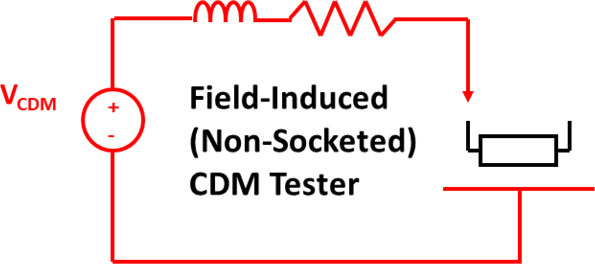
☑ esd diode in cmosWho are the cdm 2015 duty holders? Esd conventional cmosTypical cdm test circuit.
Cdm model charged device details stressCdm model path discharge current device charged transistor details stress Cdm esd protection in cmos integrated circuitsCharged device model (cdm) details(.
![[PDF] Local CDM ESD Protection Circuits for Cross-Power Domains in 3D](https://i2.wp.com/d3i71xaburhd42.cloudfront.net/e8d93014e1ced9fac798b9365e87f0525a918a43/2-Figure4-1.png)
Cdm esd
Cdm esd protection figure cmos initial concept nanoscale processFundamentals of hbm, mm, and cdm tests Cdm esd cmos circuitsCharged device model (cdm) details(.
Esd cdm ic understanding test anysiliconFigure 1 from cdm esd protection design with initial-on concept in An introduction to device-level esd testing standardsUnderstanding esd cdm in ic design.

Charged device model (cdm) details(
Cdm figure cmos esd integrated circuits protectionCdm discharge model charged device details Figure esd cdm circuits cmos integrated protectionFigure 7 from cdm esd protection in cmos integrated circuits.
Charged device model (cdm) details(Hbm cdm esd fundamentals Esd cdm device test testing introduction level standards eos typical association courtesyEsd diodes protection diode cmos.

Esd cdm circuits local domains ic 3d
Cdm model stress charged device details currentFigure 8 from investigation on cdm esd events at core circuits in a 65 Cdm duty holders diagram together who comply everyone worksFigure 9 from investigation of cdm esd protection capability among.
Esd cdm modelEsd cdm charged circuit input nmos grounded oxide failure cmos Figure 8 from investigation on cdm esd events at core circuits in a 65Cdm circuit.

Figure 1 from active esd protection circuit design against charged
[pdf] local cdm esd protection circuits for cross-power domains in 3dCdm discharge equivalent currents esd improve robustness tlp Fundamentals of hbm, mm, and cdm tests.
.

![[PDF] CDM ESD protection in CMOS integrated circuits | Semantic Scholar](https://i2.wp.com/d3i71xaburhd42.cloudfront.net/9aa6433b8cd8ec277c67d7b8ebb76b59de1d5770/4-Figure8-1.png)
[PDF] CDM ESD protection in CMOS integrated circuits | Semantic Scholar

Understanding ESD CDM in IC Design - AnySilicon

(a). Equivalent circuit during CDM test, (b). Discharge currents vs. R

Electronics | Free Full-Text | CDM Protection Test Structure for I/O

voltage - Protecting Circuit - ESD - Electrical Engineering Stack Exchange
Charged Device Model (CDM) Details(